ComparePrinted Circuit Board Assembly (PCBA)
Printed Circuit Board Assembly (PCBA): A Comprehensive Guide
Printed Circuit Board Assembly (PCBA) is the precise process of mounting electronic components onto a fabricated PCB through solder paste deposition, Surface Mount Technology (SMT), reflow soldering, rigorous inspection, and final functional testing. At Shenzhen Woke Electronics, we prioritize a strictly controlled assembly workflow to guarantee electrical performance, long-term reliability, and optimal manufacturing yields.

PCBA Services at Shenzhen Woke Electronics
As a premier Electronic Manufacturing Services (EMS) provider, Woke Electronics integrates component sourcing, high-precision SMT, and advanced testing into a single, seamless ecosystem. Our streamlined workflow is designed to help engineers and hardware startups transition from CAD designs to retail-ready hardware with maximum efficiency.
Consistent assembly quality directly correlates to superior circuit performance. This is why Woke Electronics emphasizes process control at every stage. Every step is executed by highly qualified technicians using state-of-the-art machinery to ensure world-class results.
The Woke Electronics Assembly Workflow
Technical Review: Our engineering team confirms all design files and order specifications.
Stencil Fabrication: High-precision SMT stencils are manufactured to ensure perfect solder application.
Machine Programming: Our engineers program the SMT lines using the Bill of Materials (BOM) and Centroid files (CPL) before materials even arrive.
Kit Audit: Upon receipt of materials, our team performs a comprehensive audit to resolve any discrepancies in quantity or part numbers before assembly begins.
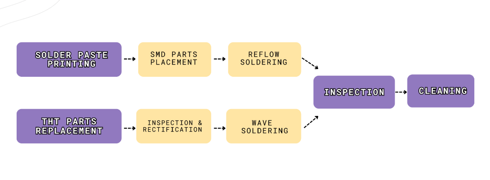
SMT Placement: Surface mount components are assembled using high-speed automated equipment. The “First Article” undergoes a strict quality check for polarity and placement accuracy.
Reflow & AOI: Boards pass through optimized reflow ovens. Upon exiting, they are immediately inspected via Automated Optical Inspection (AOI).
X-Ray Inspection: For boards with BGA or QFN components, X-ray technology is used to verify hidden solder joints and detect bridging.
DIP & THT Assembly: Through-hole components are inserted and soldered manually or via selective soldering machines, depending on the design complexity.
Cleaning & Final QA: Boards are cleaned (when required) and undergo a final high-standard quality assessment.
Packaging: Finished PCBA units and remaining materials are professionally packed for secure global shipping.
Essential Files for PCBA Orders
To ensure a flawless assembly process, the following documentation is required:
Gerber Files: Defines all PCB fabrication layers (copper, solder mask, silkscreen, etc.).
Bill of Materials (BOM): An Excel document listing all components, manufacturer part numbers, descriptions, and quantities.
Component Placement List (CPL): Also known as a Pick & Place (P&P) or Centroid file. It provides the X-Y coordinates, rotation, and side (Top/Bottom) for every component.
Step-by-Step Assembly Process
Step 1: Parts Preparation
Woke Electronics manages a robust supply chain. Components are sourced based on your BOM and prepared for the feeders. We support a wide range of parts, from ultra-fine 01005 SMD components to complex Through-Hole (THT) connectors.
Step 2: Solder Paste Application
The process begins with the application of solder paste onto the PCB pads using a precision stencil. This ensures the exact volume of solder is present to create a reliable bond.
Step 3: Solder Paste Inspection (SPI)
Every board is analyzed by SPI machines to evaluate the volume, height, and alignment of the solder paste. Early detection of paste issues prevents 70% of potential assembly defects.
Step 4: Component Pick & Place
Using advanced robotic arms, components are picked from feeders and placed onto the solder paste at high speeds. Our machines use vision systems to ensure every part is aligned perfectly with the PCB pads.
Step 5: Reflow Soldering
The boards enter a multi-zone reflow oven. The temperature is gradually increased to melt the solder paste and then cooled to create permanent, high-strength electrical and mechanical joints.
Step 6: Post-Assembly Inspection
We utilize three layers of inspection:
AOI: For 2D surface defects and polarity.
X-Ray: For hidden joints under BGAs.
Manual Inspection: For a final human-centric review of complex connectors or custom modifications.
Step 7: Final Testing & Validation
To ensure 100% functionality, we offer:
In-Circuit Testing (ICT): Checks for shorts, opens, and component values.
Functional Testing (FCT): Powering the board to simulate its real-world application.
Burn-in Testing: High-temperature stress testing for mission-critical hardware.
Step 8: Final Assembly & Packaging
Once verified, the PCBAs are integrated into enclosures (if required), labeled, and vacuum-sealed in anti-static packaging for transit.
Why Choose Woke Electronics?
From small-batch prototyping to high-volume production, Shenzhen Woke Electronics provides a one-stop solution from design to delivery. Our commitment to quality and transparency makes us the preferred partner for engineers worldwide.
Would you like me to help you draft a specific “Request for Quote” (RFQ) template to send to your clients based on these steps?
Step 6: Post-Assembly Inspection
We utilize three layers of inspection:
AOI: For 2D surface defects and polarity.
X-Ray: For hidden joints under BGAs.
Manual Inspection: For a final human-centric review of complex connectors or custom modifications.
Step 7: Final Testing & Validation
To ensure 100% functionality, we offer:
In-Circuit Testing (ICT): Checks for shorts, opens, and component values.
Functional Testing (FCT): Powering the board to simulate its real-world application.
Burn-in Testing: High-temperature stress testing for mission-critical hardware.
Step 8: Final Assembly & Packaging
Once verified, the PCBAs are integrated into enclosures (if required), labeled, and vacuum-sealed in anti-static packaging for transit.